On Monday in Shanghai, He Tingbo — president of Huawei’s semiconductor business and chair of its Scientist Committee — stood in front of a room at the IEEE International Symposium on Circuits and Systems and told the industry it had spent six decades optimizing for the wrong thing.[1] Her keynote, “New Semiconductor Path in Practice,” proposed retiring the principle that has organized the entire business since 1965: shrink the transistor, double the count, repeat. In its place, she offered the “Tau (τ) Scaling Law” — already nicknamed “Her’s Law” by her peers — which optimizes not for how small a transistor is but for how fast a signal moves through the chip.[2] “I used to think it may take us 10 years,” she told the room, “but six years, we are here.”[1]
The French wire that crossed my desk called it “un nouveau mode de fabrication de puces” — a new way of manufacturing chips.[3] It is not. That distinction is the entire story, and getting it wrong is how a reader ends up either over- or under-pricing what just happened.
Huawei did not announce a manufacturing breakthrough. It announced adesignbreakthrough, executed on the manufacturing it already has. The company is process-constrained: its chips lean on SMIC’s roughly 7-nanometre-class nodes, several generations behind the 3nm-class processes feeding Apple, Qualcomm, and AMD — and behind the 2nm that TSMC is now ramping.[4] What it claims to have built is a way to extract frontier-class transistor density from trailing-edge fabrication — by changing the layout, not the lithography.
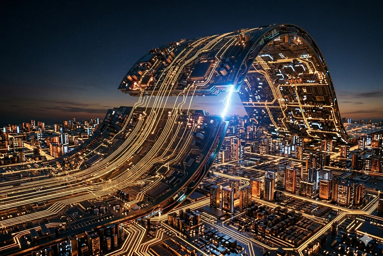
The mechanism is calledLogicFolding. In a conventional layout, logic blocks sprawl across a mostly flat plane. The limiting factor is increasingly not how fast the transistors switch, but how long it takes a signal to cross the long, resistive wires between them — a delay that caps the clock and wastes energy driving the interconnect. LogicFolding “folds” the logic — expanding the layout from one layer to two — pulling critical paths closer together, shortening the wiring, cutting propagation delay, and packing more transistors into the same footprint.[5] Huawei says the fall 2026 Kirin gains 53.5% in transistor density, to 238 million transistors per square millimeter, alongside a 40% jump in performance-core power efficiency and a 3.1GHz top clock.[6] That density figure sits, on paper, near Intel’s 18A and TSMC’s 3nm.[7] The phone is only the showcase: Huawei frames the same time-scaling logic running up through its UnifiedBus interconnect to the AI clusters, where it is trying to displace Nvidia.[8]
This is neither vaporware nor a triumph — it is a genuine engineering idea aimed at a real bottleneck. The honest steelman comes from Omdia’s semiconductor research director, He Hui, who calls it a shift from node-driven scaling to “system-level efficiency scaling”—in his view, a credible way to wring more performance out of constrained lithography.[9] Interconnect delay is genuinely the dominant frontier problem, and stacking silicon to address it is not new: HBM has stacked memory since 2015, and TSMC and Intel have stacked finished dies with SoIC and Foveros. What Huawei claims is harder and less proven — folding a single logic block’s own gates across two bonded tiers so signals take a short vertical hop instead of a long planar route. That is logic-on-logic at the cell level, the territory the whole industry has been circling for a decade, because the thermal and yield problems are brutal. The difference from the rivals’ version is that theirs still rides on leading-edge fabs Huawei cannot buy.
But density on a slide is not density at competitive yield, power, and thermals. The most important sentence published all day came from Paul Triolo of DGA Group: a stacked or folded design can produce genuine density gains, he said, but it “does not mean Huawei has solved” the yield, power, thermal, and device-performance problems of true 1.4nm-class manufacturing.[10] Counterpoint’s Neil Shah was blunter on the strategic point: this “parallel semiconductor path is still unproven at scale.”[11] And the headline number — a transistor density “equivalent to” a 1.4nm process — is not a 2026 result. It is a 2031 projection, unaccompanied by any independent performance data.[12] Stacking buys you density. It does not automatically buy you the efficiency that makes density useful at the frontier.
So strip the projection away and look at what actually shipped: a strategic reframe. The export-control regime was architected on the premise of manufacturing. Deny China extreme ultraviolet lithography — the ASML machines no Chinese firm can legally buy — cap it at 7nm, and the density frontier stays out of reach.[13] The wall is real, and it works against the thing it was built to stop. What it cannot do is stop Huawei from deciding that the frontier is no longer defined by the dimension the wall measures. If the goal is signal-propagation time rather than transistor pitch, then a control regime denominated in nanometres is policing a metric the target has stopped competing on. Even Triolo, who doubts the manufacturing claim, reads the move this way: Huawei is “turning an engineering strategy into a quasi-’law’” — shorten wires, stack logic, co-design the whole system.[10]
The reframe does not entirely escape the wall. A folded design still has to be finalized for production on EDA software, where America’s Synopsys and Cadence dominate, and fabricated on SMIC’s constrained base node. Huawei now claims home-grown design tools, but domestic EDA at the leading edge is unproven — and Washington showed in 2025 that it can switch the EDA tap off at will, before it relented.[13] The dependency is real. It simply no longer sits where the lithography rules are pointed.
The market saw the same thing even where the engineering is unproven: SMIC shares rose 7.6% on the news.[14] And the competitive backdrop sharpens it — last week, Nvidia’s Jensen Huang told CNBC his company had “largely conceded” China’s AI chip market to Huawei.[15] The Tau Law is a flag planted in the ground that Nvidia is vacating.
None of this means Huawei has closed the gap. It almost certainly has not, and the skeptics may be entirely right that folding logic across bonded tiers hits a thermal-and-yield ceiling well short of the 2031 target. But the bet is now legible, and it is falsifiable on a clock. The first checkpoint is this autumn, when the new Kirin ships and an independent teardown can confirm or puncture the density claim. The test is not whether the design works on a slide but whether Huawei can build it in volume without the chips failing — the gap, in stacked designs, where ambition usually dies.[16] The second checkpoint is 2031. If either one lands at competitive efficiency without EUV, Washington is left writing its rules in a unit that no longer measures the race.
The wall was built to keep China from making the transistors smaller. Huawei’s answer is to stop trying.
Notes
[1]: He Tingbo delivered the keynote “New Semiconductor Path in Practice” at the 2026 IEEE International Symposium on Circuits and Systems (ISCAS), Shanghai, May 25, 2026. Huawei newsroom, “HUAWEI Presents the Tau (τ) Scaling Law, Enabling Breakthroughs in Transistor Density and System Performance,” May 25, 2026,huawei.com. Vendor-primary source. The “I used to think it may take us 10 years, but six years we are here” remark, and a teaser that Huawei would “bring the surprise” before winter 2026, are reported from the keynote by BusinessToday,businesstoday.in.
[2]: The principle “proposes replacing geometric scaling with time (τ) scaling as a new guiding principle for the evolution of both semiconductors and electronic systems.” Huawei newsroom, ibid. The “Her’s Law” nickname (a play on He Tingbo’s surname and the convention of naming foundational laws after their originators, as with Moore’s Law) is reported by the South China Morning Post, “Huawei unveils new scaling law and tech that narrows gap with TSMC, Samsung,” May 25, 2026,scmp.com. τ (tau) is the time constant engineers use to describe how quickly signals propagate through a circuit.
[3]: “Huawei a développé un nouveau mode de fabrication de puces,” Boursorama (reproducing an AFP wire), May 25, 2026,boursorama.com. The “fabrication” framing is the error this piece corrects.
[4]: On the process gap: “analysts say China remains behind global leaders in the most advanced process technology,” with Huawei’s chips produced on SMIC’s 7nm-class node versus TSMC’s 2nm. Reuters, “China’s Huawei reveals chip design breakthrough amid US sanctions,” May 25, 2026,reuters via rappler.com. The Kirin 9030 (Mate 80 Pro Max) was built by SMIC on an “N+3” process, a scaled evolution of its 7nm node and still behind TSMC and Samsung, per a TechInsights teardown reported by the South China Morning Post,scmp via tech.yahoo.com.
[5]: LogicFolding “would shorten wiring inside chips and considerably improve performance”; Reuters, op. cit. (rappler.com). Huawei’s own description: the architecture “can be used to continuously compress signal propagation delay and steadily improve transistor density.” Huawei newsroom, op. cit. CNBC reported that “Huawei’s new chip architecture expands the layout from one layer to two,” per He Tingbo. CNBC, “Huawei plans new smartphone chips this fall,” May 25, 2026,cnbc.com.
[6]: Per-metric figures (vs. a conventional SoC): +53.5% transistor density to 238 MTr/mm², +40% P-core power efficiency, and +12.7% max clock frequency to 3.1GHz. These figures appear in He Tingbo’s ISCAS presentation slides as relayed by trade press; they are not stated in Huawei’s official press release, which carries only the τ Law framework, the “381 chips” and “Fall 2026 Kirin” claims, and the 2031 target (Huawei newsroom, op. cit.). Slide figures via FoneArena, “HUAWEI presents Tau (τ) Scaling Law,” May 25, 2026,fonearena.com, and Huawei Central,huaweicentral.com. Vendor-claimed presentation data; no independent verification as of publication.
[7]: The 238 MTr/mm² figure has been described as roughly comparable to Intel’s 18A and TSMC’s 3nm-class density. The comparison is density-only and does not establish equivalent power, yield, or performance; nor is it specified whether the figure is logic-only or SRAM-inclusive, which materially affects any cross-foundry comparison. Treat as vendor-claimed slide data pending an independent teardown of the shipping Kirin.
[8]: Huawei describes the τ Scaling Law operating “at the system level” by “redefining interconnect protocols for computing systems with UnifiedBus to achieve unified memory addressing and native memory semantics for SuperPoDs,” reducing system communication latency. Huawei newsroom, op. cit. (huawei.com). This situates the phone-level LogicFolding claim within Huawei’s broader AI-cluster ambition.
[9]: He Hui, director of semiconductor research at Omdia, quoted in Reuters via Rappler, “China’s Huawei reveals chip design breakthrough amid US sanctions,” May 25, 2026,rappler.com.
[10]: Paul Triolo, head of technology, Asia and Americas, DGA Group, quoted in CNBC, “Huawei plans new smartphone chips this fall as rivalry with Nvidia and Apple heats up,” May 25, 2026,cnbc.com. Full quotes: “A stacked/folded design can produce effective density gains, but it does not mean Huawei has solved the full process, yield, power, thermal, and device-performance problems associated with true 1.4 nm-class manufacturing”; and separately, “Huawei is turning an engineering strategy into a quasi-’law,’” which Triolo characterized as “more a systems-level optimization doctrine: shorten wires, stack logic, improve memory semantics, and co-design chips, packages, software, and clusters.”
[11]: Neil Shah, vice president of research, Counterpoint Research, quoted in CNBC, ibid.
[12]: “By 2031, the high-end chips HUAWEI designs based on the τ Scaling Law are expected to feature a transistor density that is equivalent to 14 Å (1.4 nm) processes.” Huawei newsroom, op. cit. “Although Huawei did not provide independent performance data, the target is significant because 1.4 nm is expected to be close to the global frontier for advanced chipmaking around the end of the decade.” Reuters via Investing.com,investing.com.
[13]: China “is widely seen as unlikely to reach that level through conventional manufacturing alone because Washington has restricted its access to advanced lithography tools and other key semiconductor technologies.” Reuters, op. cit. ASML has never shipped an EUV machine to China, and there is no credible domestic alternative — the binding reason SMIC sits several generations behind TSMC and Samsung; see TheNextWeb, “Huawei unveils ‘Tau Scaling Law’ as China’s workaround,” May 25, 2026,thenextweb.com. On the EDA dependency as a demonstrated lever: US BIS ordered Synopsys, Cadence, and Siemens EDA to halt China sales in late May 2025, then rescinded the restriction on July 2, 2025; the three firms hold roughly 80% of China’s EDA market. US Commerce/BIS via Network World, July 3, 2025,networkworld.com; EE Times,eetimes.com. The episode established that the tool dependency is a switch that can be activated, even though it is not active as of publication. At the keynote He Tingbo claimed Huawei had spent six years building domestic capabilities “including electronic design automation (EDA) tools and chip design methodologies”; BusinessToday, May 25, 2026,businesstoday.in. Domestic EDA at leading-edge nodes remains commercially unproven.
[14]: SMIC shares rose 7.6% on Monday following the LogicFolding announcement. South China Morning Post, op. cit.; Reuters via Rappler, op. cit.
[15]: Jensen Huang told CNBC the company had “largely conceded” China’s AI chip market to Huawei. CNBC, op. cit.; corroborated in Modern Diplomacy,moderndiplomacy.eu.
[16]: LogicFolding is described as cell-level “folding” — distributing a single logic block’s gates across two vertically bonded wafer tiers connected by hybrid bonding — rather than the die-to-die stacking used by HBM or by TSMC’s SoIC and Intel’s Foveros. One technical reconstruction puts the Kirin 2026 hybrid-bonding pitch at ~1.5µm (versus TSMC SoIC at <15µm and Intel Foveros at ~25µm TSV pitch), with density scaling roughly as the square of interconnect pitch; the same analysis back-calculates the density gain as 155→238 MTr/mm². These are independent analyst figures, not Huawei-published data: GlobalSemiResearch, “Huawei’s Tau Scaling Law: A Technical Deep Dive,” May 25, 2026,globalsemiresearch.substack.com; pitch comparisons via SemiAnalysis,semianalysis.com. The thermal and yield penalties of logic-on-logic stacking are long-documented; see Semiconductor Engineering, “Stacking Logic On Logic.”